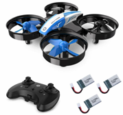
So far, so good. A simple idea resulting from the problem that the flight time of the drone is very short (~10min / battery). So you use several batteries and after the flight they all have to be recharged. With only one charger, you have to switch and it takes time to get ready to fly again. Ideally, you use a quick charger to charge one set of batteries while flying with the other. Definitely a problem of the modern luxury society – we want things out of sheer comfort, even though we don’t actually need them.
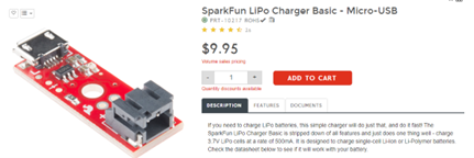
From this problem definition, one can already see the requirements of electronics, what they must be able to do, and also what are non-objectives. At this point in a project, market research is usually the next step. Is there already such a solution, which you can simply buy… and of course you can buy such a product in the form of PCB’s with USB micro connector and a charge controller chip suitable for this battery chemistry (lithium polymer) as well as the appropriate connector for the batteries.
Let’s assume that in the make-or-buy decision (for whatever reason) we decided to do the electronics development ourselves. Let’s get started!
The electronics development process comprises three phases: the design phase, the manufacturing phase and the commissioning phase. In the following, you will learn what to consider in the individual phases.
Construction phase
Definitions:
- The design shows the basic architecture of the circuit.
- The circuit diagram clearly defines the components and their connections.
- The layout clearly defines the PCB (Printed Circuit Board), it contains “footprints” for all components as well as routing paths for correct connection according to the circuit diagram.
Design/Architecture
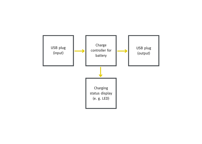
Circuit diagram
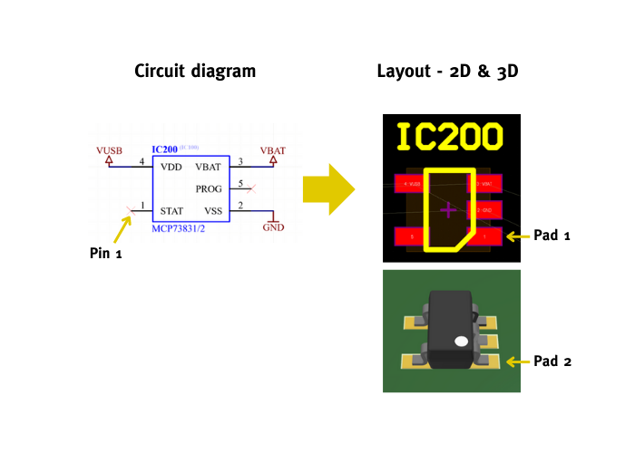
The elements from the design (blocks) are defined and placed on the circuit diagram in the form of components and connections (nets).
Component selection
The component selection happens in the course of the circuit diagram creation. Choosing the right components is sometimes the most important part of a project, because it lays the foundation.
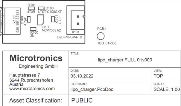
For this project, an integrated circuit is used to charge the battery.
- Manufacturer: Microchip
- Type: MCP73831
Hint: How does one decide to use exactly this component? (The criteria for component selection would go beyond the scope. We simply take the circuit diagram in this example as given).
Circuit diagram creation
The circuit diagram is created in the “schematic editor” of the ECAD Design Tool. In the current example, Altium Designer is used.
1. placing the components (from the component libraries of the ECAD Design Tool)
The components do not yet have any values and there is no electrical connection between them. If components do not yet exist, they must be drawn in advance.
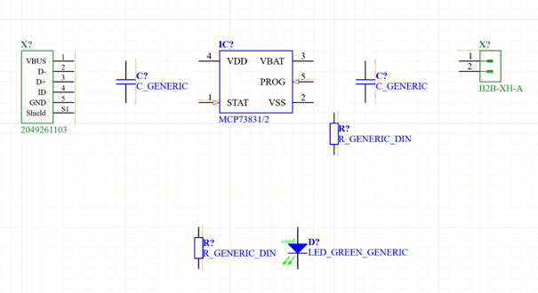
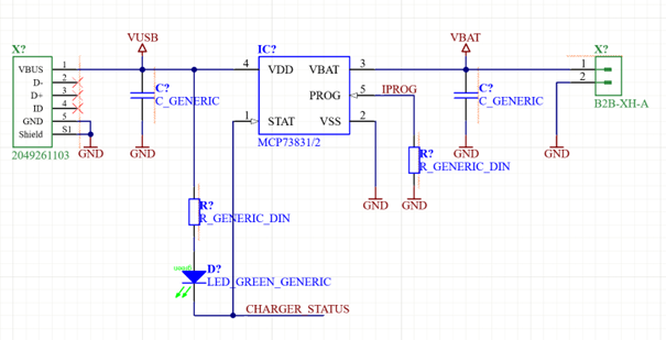
2. draw electrical connection
The tools of the ECAD Design Tool are also used here: connection lines, power ports (“VBUS” “GND”) or network names (“CHARGER_STATUS”). The pins (connections of the components) are correctly connected to each other.
3. define component values
The calculation is made according to the specification. Likewise, each component is given a unique identifier (“designator”), for example “IC100”, which may only exist once in the circuit diagram.
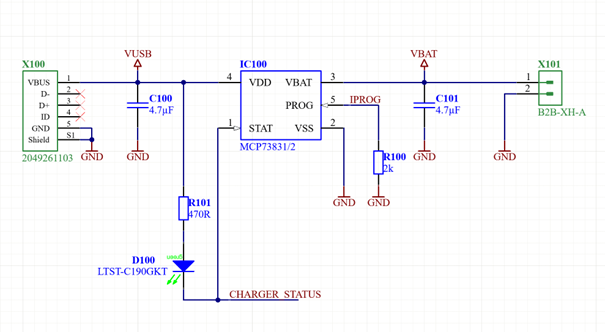
This is now a complete circuit diagram. All components are present and clearly defined. All pins (connections of the components) are connected and unused pins are marked accordingly.
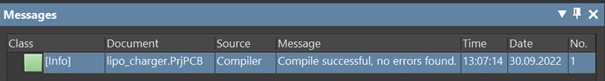
An ERC (“electrical rule check”) is carried out as proof. The ERC checks for “unconnected pins” or “single net labels”, for example, and many more points. Mainly the syntax, i.e. the correct use of the design elements of the ECAD tool, is tested.
It’s OK!
Schematic – Layout (PCB Design)
The components and connections on the circuit diagram are “transferred” to the PCB. This procedure is called “forward annotation”. This only works if the circuit diagram is drawn without errors (ERC OK). The “pads” (connections of the components) are connected accordingly, as defined in the circuit diagram. As a counterpart, there is the “backward annotation” to transfer a change to the components (values) or the electrical connection (“pin swapping”) on the PCB design to the schematic. However, this happens very rarely.
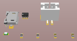
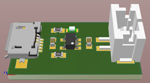
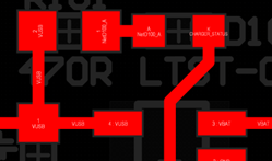
Logical components in the schematic are placed in the layout in the form of physical components (“footprints”). The integrated circuit makes it easy to see what is happening here. As PC technology and Altium designers have evolved, there is also a 3D representation:
The 3D representation of the components is all well and good, but equally useless for the PCB designer. The 3D data of the PCB helps with a mechanical fit into an enclosure (collision analysis by CAD designer), but not with the unbundling of the tracks.
Note: The schematic symbol is drawn differently than the layout symbol, which can be seen here by Pin1 –> Pad1. It is very common for these two symbols to diverge. Therefore, it is good practice to check the assignment of pin –> pad against the data sheet (“Pinout”). The difference is due to the fact that the layout symbols (“footprints”) are mostly generic and come from a different library than the manufacturers’ “schematic symbols”. This footprint here, for example, has the name “SOT23-5”, and thus fits any integrated circuit in this form factor.
Create layout
The layout is created in the PCB editor of the E-CAD design tool, in this case also in Altium Designer.
After the “forward annotation”, the footprints of the components are created in the PCB document, and the connections (as they should be) are shown in the form of thin lines.
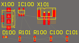
Placement & board size
The components are arranged in such a way that the unbundling is possible without crossings. Then a board size is defined. In this case, make sure that the micro-USB connector housing protrudes beyond the circuit board (otherwise the micro-USB connector on the cable will not fit in, it would touch the circuit board).
At this stage it already looks quite “pretty” but would not work because the actual work of unbundling has not happened yet.
Note: The placement rule “as free of crossings as possible” comes from a time when crossings had to be made in the form of soldered wire bridges. With boards as simple as this one, you can still follow the same procedure. This results in a so-called 1-layer PCB in this case, where it is possible without crossing. However, a complex mixed-signal PCB design has significantly more complex component placement rules, and also significantly more layers (6 or more).
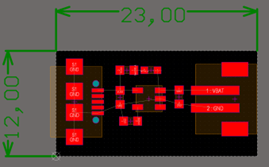
Unbundling (Layouting)
Unbundling is trivial in this case. With complex boards, high component density and many layers (mainboards), routing is a very time-consuming process.
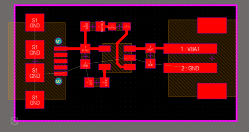
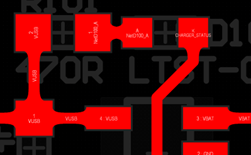
I would like to discuss a mechanic that is common practice today. As you can see, the entire “GND” network is (intentionally) not routed.
It is defined in the E-CAD design tool that the remaining PCB area is used for GND (“GND polygon”).
The ECAD tool automatically connects the remaining “GND pads”, using four connections (“centres”) each, if possible.
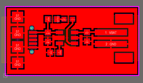
At this point, the layouting is complete. The DRC (“Design Rule Check”) is carried out as a check. The layout is checked on the basis of the design rules. If errors or warnings are found here, the board must not go into production!
It’s OK!
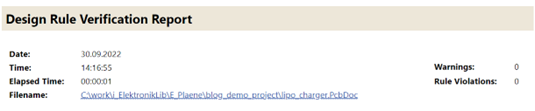
Note: With the DRC, of course, it is only possible to check against the design rules. These must be properly adjusted in advance – to suit the design. If, for example, a “short circuit” is allowed by design rule, all “short circuits” are OK for the DRC (of course, this must not be done).
Layout cosmetics
Making the layout “beautiful” can be a very time-consuming process. It is a personal requirement that you have as a PCB designer that your own creation looks appealing. A standard that most craftsmen should have. What you can imagine by this: Arrange the pathways well, lead them parallel, round them off, align them centred, symmetry,…
Altium Designer offers a “teardrop” feature that rounds out pad inputs. In fact, however, it has little to do with cosmetics, even if it looks very pretty. It improves pad stability (for thin conductive tracks on flexible PCBs). The “teardrop” is also used for vias, where more copper remains. It helps if the hole has a slight positional deviation, i.e. is not drilled exactly via-centre, but should be. In the current design there are no “vias”, but you can also see very well on the pads what “teardrops” look like.
Manufacturing data
There are two sets of data needed for the production:
- Circuit board production („fabrication outputs“): contains the data for the production of the blank
- Electronics assembly (“assembly outputs”): contains the data for the assembly and soldering of the components.
Before the production data is created, the service prints and the assembly plan should be created. These two points are optional and not relevant for the actual function of the board. However, it is good practice to deliver a proper craft.
Assembly plan
This is a printed plan designed to answer the question, “What is where on the PCB ?”
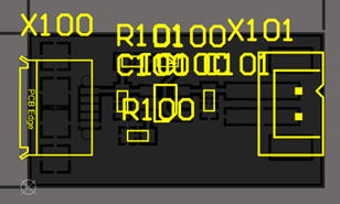
As the graphic shows, only the “designators” are shown. This is basically sufficient, as the “schematic” allows you to clearly assign the component type. If you can arrange it, component type/values “comments” should also be recognisable on the placement plan. This makes it easier for manual assembly, as you then only need the assembly plan and not the circuit diagram.
A good placement plan is characterised by good legibility (printed on paper). The texts should not be too small. The “stroke font” used here is historically but still frequently used. This is a font with a constant line width, from a time when these plans were printed by plotters. Nowadays, there is nothing to be said against using a “true-type font”.
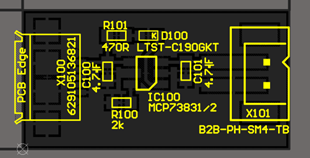
Here you can see the component plan with “designator” and “comment” – displayed for clear component identification.
Service printing
This refers to elements printed on the circuit board. In the past, it was common to print the “designators” on the PCB. This meant that components could be clearly identified on the finished PCB – even without the assembly plan.
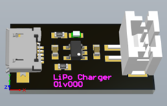
Whether you want to do that or not is up to the designer. One possibility for this PCB would be, for example, to write down the name and version identifier.
PCB cosmetics
“There are also other colours than green…”
The board colour is usually the colour of the solder-stop lacquer (“solder-stop”). Usually the whole board is covered with “solder-stop”. Without this lacquering, the boards would be rather yellowish, depending on the base material used – but mainly “FR-4” is used. The “solder-stop” results in the classically known colours as they are known from circuit boards today. The colour green is still the most common.
There is also a limited choice of colours for the service print (“silk screen”).
Both are features of the board manufacturers. Colour variations are to be expected across different delivery lots and manufacturers.
Fact: Green “solder-stop” and white “silk-screen” are the standard.
But there are other ways:
Create manufacturing data
„Fabrication outputs“ > PCB
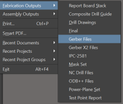
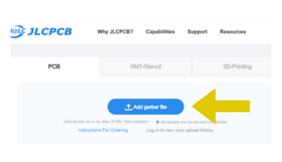
So-called “gerber files” are required for the production of the circuit board. This is a very old data format. The data is usually uploaded as a zip archive to a PCB manufacturer.
Gerber files have defined file extensions. “Defined” here means that the board manufacturers expect a specific format of what content is in what files. If you want to have a “service print”, you should make sure that it is included in the “.GTO” file. Otherwise, it can happen that something else is printed on the PCB than you actually wanted. The PCB outline is mostly expected to be “.GM1” or “.GKO”.
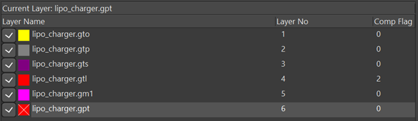
Normally, however, there is little need to worry about the correct file extensions. The ECAD Design Tool usually gets it right.
Nevertheless, it is good practice to check the generated “gerber files” manually before transferring them to the PCB manufacturer.
Manufacturing data „assembly outputs“ > PCB-A
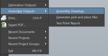
The “pick & place” files are required for machine production. These contain the X/Y coordinates of each component and are required by placement machines for fully automatic component placement.
For a manual assembly, the “assembly drawing” (=assembly plan) is needed, which we have drawn so beautifully before.
A Microtronics assembly plan also contains a “document header” – as is usual with technical drawings.
Manufacturing phase
Depending on the quantity and type of PCB, a decision is made between in-house and external production. “As a child of the 80s, I still had the pleasure of making the circuit boards myself during my apprenticeship. Starting with the cutting, the exposure process, the etching away of excess copper with FeCl3 (iron-III-chloride) up to the drilling. The finished board was then assembled by hand, the connecting wires of the components were soldered with a soldering iron and the protruding wire was shortened with a side cutter,” Stefan remembers.
Circuit board manufacturing
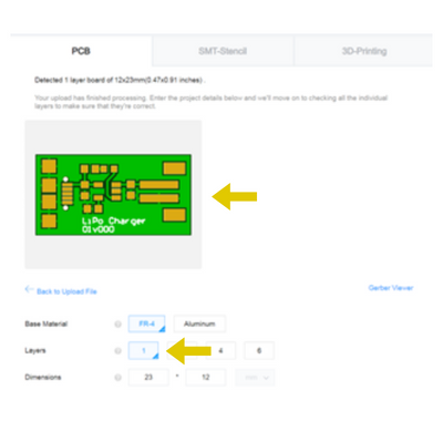
In 2020, the circuit boards have already been ordered online (but not yet on Amazon). There are a variety of producers with online platforms (e.g. JLCPcb.com).
The “assembly outputs” gerber data are compressed and uploaded in a zip archive.
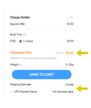
In the preview, the board appears as we have drawn it. The PCB properties are already recognised automatically for the most part on the basis of the encoder files. Here, too, all order data are checked. The PCB price appears and then you can finally press the “Buy Now” button.
Attention: PCB manufacturers in the Far East like JLCPcb.com are – compared to the EU – very cheap. For this, higher shipping costs and longer shipping times apply.
Ex: 2 € PCB (5 pieces) and 20 € shipping (UPS 5 days)
Another trend in PCB manufacturing is that small quantities are exorbitantly expensive. The example of JLCPcb.com – by modifying the number of pieces – shows this very well.
| Qty | Ext Price [€] |
| 5 | 2,00 |
| 10 | 5,01 |
| 100 | 10,22 |
| 1k (1000) | 20,14 |
| 10k | 119,65 |
| 80k (highest possible) | 894,07 |
The main price driver for small quantities is the manufacturing technology of the PCB, i.e. how many process steps the PCB manufacturer requires. Small quantities of so-called HDI (high technology) circuit boards can be in the price range of a few 1,000 euros.
In mass production, the biggest price driver is PCB size followed by the number of layers and copper thickness. In other words, it is the material quantity-defining component that has the greatest impact in mass production.
The factors are easy to “explore” using the example from JLCPcb.com, if you play with the board parameters in a self-experiment and look at the price development.
Component order
The components are purchased on the basis of the “Bill of Materials” (BOM). This is mostly an (Excel) list. The BOM is already defined in the course of creating the circuit diagram.
For this project, the parts list is very lean:
- 7 different components – Variance = 7
- 8 components in total – Quantity = 8
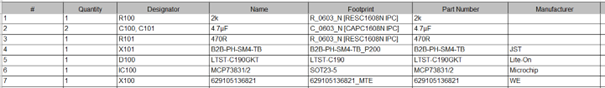
Component variance is a factor that comes into play in series production. Therefore, it is more common in larger PCB designs to assemble a particular component value from two others to reduce variance at the expense of component quantity. In series production, components are purchased on reels. These rolls can quickly contain around ten thousand pieces.
Components for DIY projects are usually bought online from various catalogue retailers (e.g. RS-components, mouser, aliexpress, …).
PCB assembly
This PCB can still be equipped manually.
At Microtronics, circuit boards of this type are assembled by hand for simplicity’s sake. Solder paste is applied using a soldering template and a spatula (squeegee). The components are hand-assembled with tweezers and a microscope if they are very small. The assembled board goes into a small soldering oven. This passes through the solder profile in a controlled manner (heating up to ~220°C). In the past, Microtronics (no kidding) used an electric pizza oven for this purpose.
Commissioning phase
Have we done everything right?
In this case we will find that the polarity of the battery plug does not match. Plus and minus are reversed, so we have to rework this manually. The repair looks, for example, like bending the connection pins of the battery connector to the other side and re-soldering it.
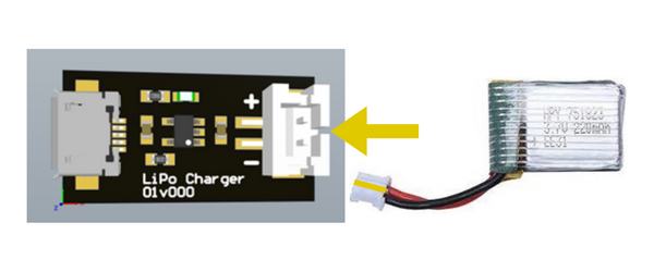
Here in the pictures you can see the coding of the connector and connector housing. When you plug it together, the red cable ends up on minus.
Definition: The aim of the prototype is to prove that the idea works (“proof of concept”).
A prototype does not have to work smoothly. It is perfectly OK if it contains errors and does not run smoothly.
Next Steps?
In the case of a DIY project, it ends here. In this case, the PCB with the reworked plug will then already be sufficient to fulfil the “need”.
For a product that is supposed to end up on the market later, the fun is just beginning here!